Let's put the etch factor aside for a moment. First, let me ask you a simple question: a transmission line is designed with a rectangular cross-section. What shape do you think it becomes after being manufactured by a PCB fab?You Say Rectangle, But What Are We Really Talking About?
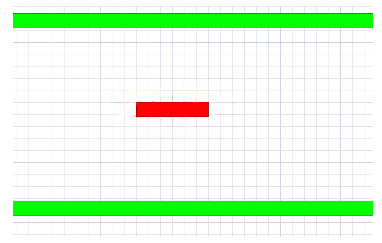
For most PCB design engineers, their focus is on the layout. For a simple transmission line, if the trace width and copper thickness are set to specific values in mils, that's what they design to. They assume the final fabricated trace will look like the 3D model of an inner-layer trace below, and in cross-section, this transmission line is a perfect rectangle!
Ideals are one thing, but reality is often another. After this transmission line is sent to a PCB fab for manufacturing, is it still that perfect rectangle? Let's first look at the PCB fabrication process to see how this trace is actually made.
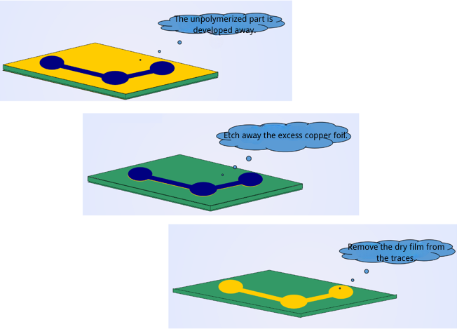
For fabricating inner-layer traces, the core step involves using the developing function of a dry film to guide a chemical solution in etching away unwanted copper, leaving only the desired circuit traces.
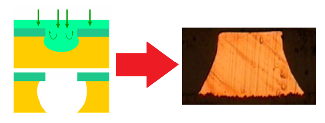
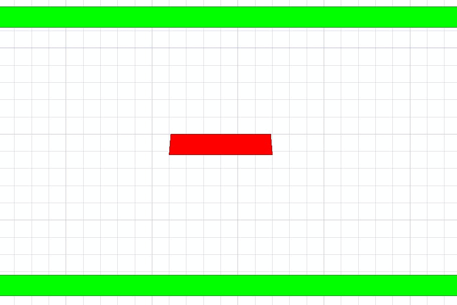
But a problem arises during the etching process. Because the chemical solution is highly fluid, the etching doesn't happen uniformly. To put it simply and visually, the copper at the top gets etched more thoroughly than the copper at the bottom. As a result, the cross-section of the final trace looks like the diagram below.
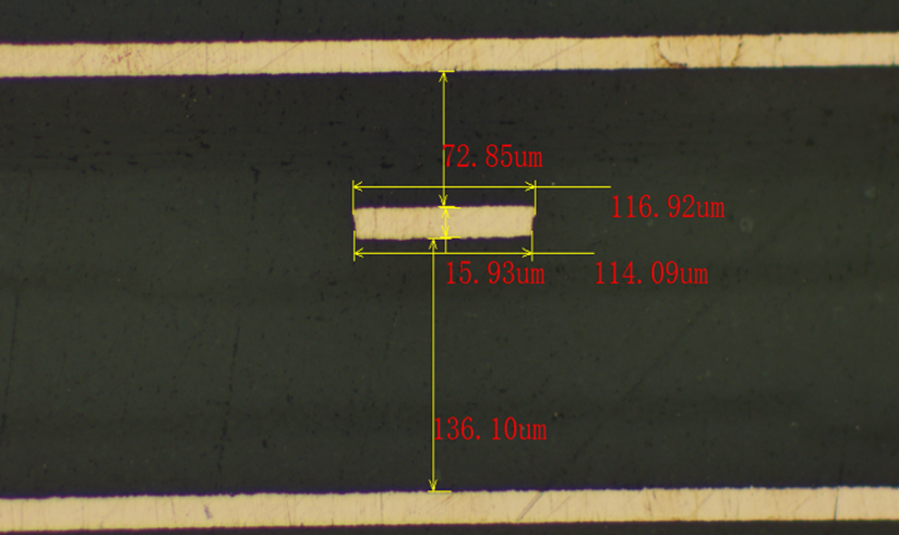
What?! So you're saying the ideal rectangular trace becomes a trapezoid after fabrication? Is there a formula to quantify the shape of this trapezoidal trace? You bet there is. This brings us to the topic we've been building up to: the Etch Factor! Its official definition is as follows.
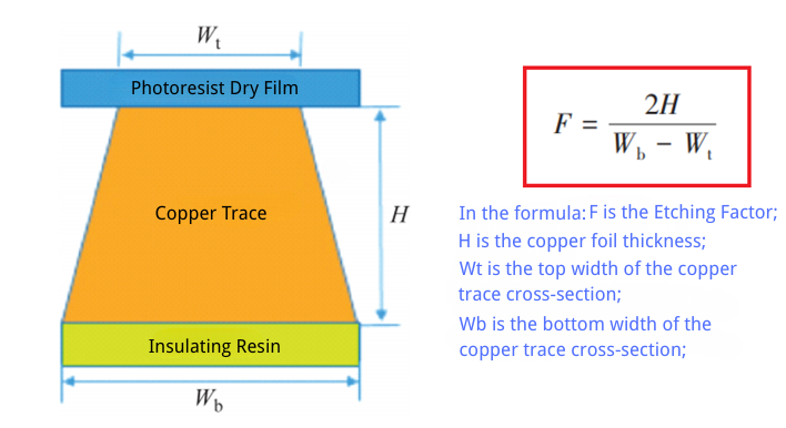
In simple terms, it measures the difference between the top and bottom trace widths after etching. Based on the ideal rectangular shape, the smaller the difference between the top and bottom widths, the better. In other words, a larger etch factor (F) is better. A higher etch factor indicates a fab's superior etching capability!
Alright, that's enough about the fabrication process for now. If you're interested in more, you can talk to "Dong Ge." So, let me (Chris) talk about how much of an impact the etch factor has on impedance control. We'll share some insights by comparing some 3D transmission line simulations.
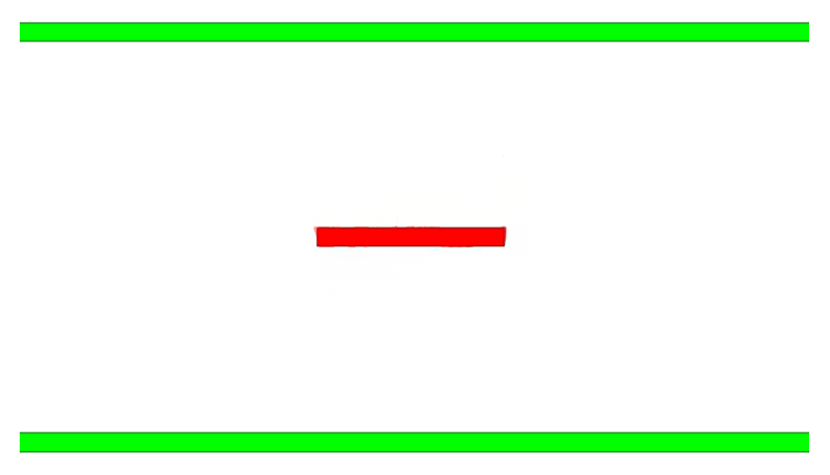
First, let's look at a 50-ohm single-ended line model with a trace width of 6 mils, as shown below:
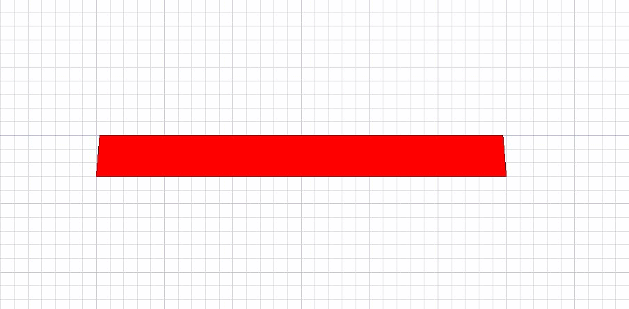
Now, let's simulate the change in trace shape for different etch factors, as shown in the animation below. It starts from an ideal infinite etch factor (a perfect rectangle), then goes to an etch factor of 12, and gradually decreases to 2.
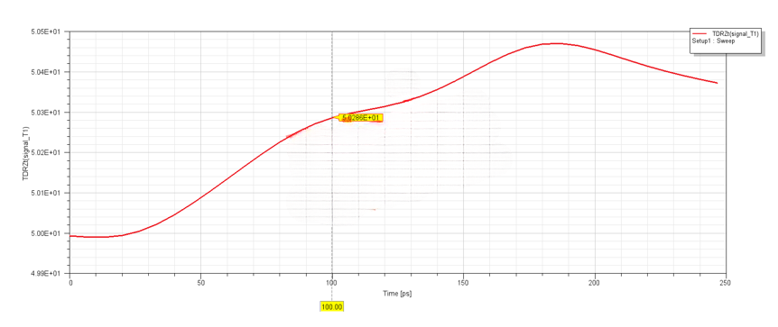
For the ideal rectangle, the impedance is exactly 50 ohms, as shown below:
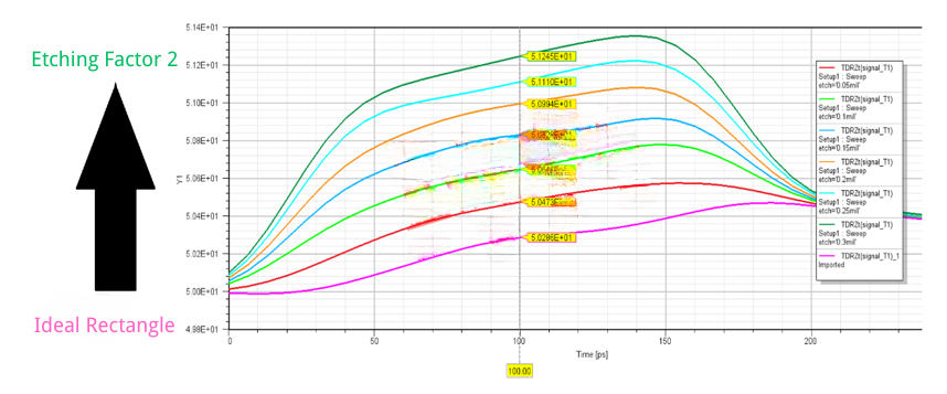
Now, let's put the impedance changes for different etch factors on a single chart. Here's what it looks like:

From 50 ohms for the ideal rectangle to 51.2 ohms for an etch factor of 2, the impedance error is 1.2 ohms! That's an error of 2.4% from this etching step alone!!!
Think that's not a big deal? Let's see what happens with a trace that is only 3 mils wide. The image below shows an ideal 3-mil, 50-ohm transmission line.
Now let's compare the impedance change with the same variation in etch factor. Here's the animation:
With the same change in etch factor, the impedance change for the 3-mil trace is undoubtedly more dramatic, going from 50 ohms for the ideal rectangle to 52.2 ohms for an etch factor of 2.
A quick calculation shows that with an etch factor of 2, the impedance is 52.2 ohms. The fabrication error from this step alone reaches 4.4%. And remember, the etch factor is just one of many steps in the long process of fabricating a controlled impedance board. Other steps will also introduce errors. Therefore, achieving a final impedance tolerance of 5% is not something that can be accomplished with just a little effort!
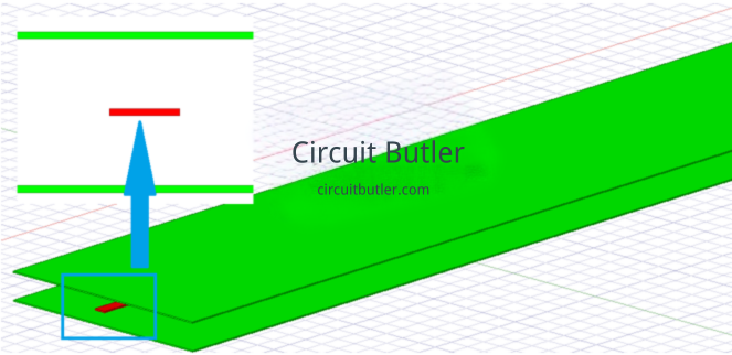
Speaking of which, we have to mention Circuit Butler, which specializes in high-end, quick-turn prototyping and provides high-quality manufacturing for high-layer-count, high-speed, high-precision, and HDI PCBs. In terms of key technical indicators, the fab can consistently achieve an impedance control accuracy of ±5%. For 20-layer PCB products, the production and delivery cycle can be compressed to as fast as 8 days, effectively meeting customer demands for high-precision and quick delivery on high-end PCB products.
A few final words. I'm sure most of our loyal followers know that we have a brand-new fab. Regarding etch factor research, I (Chris) already ran test boards to verify this right when our fab started production. I won't say more. Let's end this article by showcasing our fab's capabilities with a real-world example.