

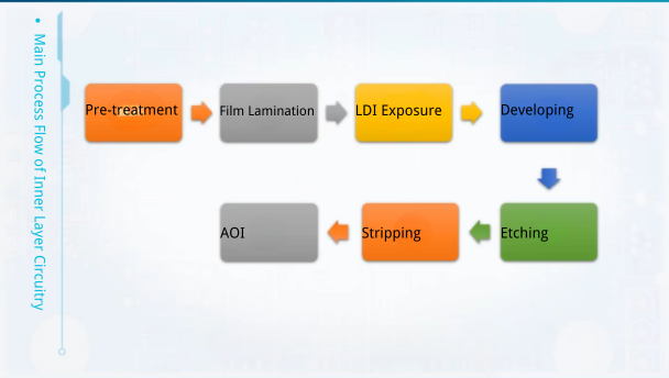
In the world of electronics, the Printed Circuit Board (PCB) serves as the foundational skeleton for all components and the intricate nervous system connecting every signal. The manufacturing of a PCB is a complex engineering feat that integrates a multitude of advanced technologies. Today, we will unveil the mysteries of its most critical stage—the high-precision inner layer patterning process—and explore the journey of transformation from a simple copper-clad laminate to the initial form of a precise circuit.
This article will focus on the first crucial half of the inner layer fabrication process: from Pre-treatment to LDI Exposure.
Step 1: Laying the Foundation – Pre-treatment and Dry Film Lamination
Every precision process begins with flawless preparation.
1. Pre-treatment
Imagine creating a masterpiece on canvas. You first need a canvas that is clean, smooth, and allows the paint to adhere firmly. The pre-treatment of a PCB follows the same principle.
Purpose: The objectives are twofold:
Surface Cleaning: To remove oils, oxides, and other impurities from the copper foil surface, ensuring a pristine base for subsequent steps.
Surface Roughening: Through a process called micro-etching, the copper foil surface is slightly corroded to create microscopic peaks and valleys. This roughened texture dramatically increases the surface area, thereby significantly enhancing the bonding strength (adhesion) of the dry film.
A perfect pre-treatment is the cornerstone of successful pattern transfer.
2. Lamination
Once the "canvas" is prepared, we apply a special "primer." This is the Dry Film.
What is Dry Film?
Dry film is a photosensitive polymer material and an essential consumable in the PCB pattern transfer process. Its magic lies in its ability to undergo a polymerization reaction (or cross-linking) when exposed to ultraviolet (UV) light of a specific wavelength. This reaction makes the molecular structure of the exposed areas incredibly stable, enabling it to resist the chemical solutions used in later etching and plating stages.
The Lamination Process:
We use a fully Automatic Film Laminator to apply the dry film evenly and smoothly onto the pre-treated copper-clad laminate, ensuring there are no air bubbles. The level of automation and precision in this step directly impacts the quality of the final circuitry.
(Image placeholder: A picture of an automatic lamination machine)
Step 2: From Blueprint to Reality – The Revolution in Pattern Transfer
After the copper-clad laminate is coated with its dry film "armor," we arrive at the most critical step: Exposure, where the designed circuit pattern is accurately "drawn" onto the dry film.
1. Traditional Exposure vs. LDI/DI Direct Imaging
In the past, pattern transfer relied on a "phototool," commonly known as film. The entire workflow was: Engineering Design -> Photoplotter outputs Film -> Exposure machine transfers the pattern from the film to the dry film.
Limitations of Film: As a physical medium, film is susceptible to dimensional instability (expansion and contraction), deformation, and scratches. It also requires a strictly controlled storage environment. These factors could all compromise the final pattern's accuracy.
Positive vs. Negative Film:
Negative Film: The pattern areas are transparent. After exposure, these areas of the dry film cure. The unexposed (non-circuit) areas are washed away during developing, exposing the copper to be etched away later. In short, what you see is what gets removed.
Positive Film: The pattern areas are opaque. The circuit areas of the dry film are shielded from light and do not cure. They are washed away during developing, revealing the copper circuitry that will remain. Today, positive film is the mainstream, embodying the "what you see is what you get" (WYSIWYG) principle.
However, technological advancements have gradually pushed film off the historical stage. The advent of LDI/DI Direct Imaging technology has sparked a revolution.
2. LDI and DI: The Dawn of a New Era
DI (Direct Imaging)
LDI (Laser Direct Imaging)
The principle behind both technologies is the same: they eliminate the need for film by using a computer to directly control a light source, which projects the circuit pattern with high precision onto the dry film.
The Key Difference: The light source.
LDI uses a laser, which is monochromatic and has concentrated energy, allowing for extremely high precision. Consequently, it has strict requirements for the color of the dry film, which must match the laser's wavelength.
DI uses a multi-wavelength or full-spectrum light source (like high-power LEDs), making it compatible with a wider range of dry film colors and offering greater versatility.
Today, direct-write technologies, led by LDI, are developing rapidly and have become the standard for high-precision PCB manufacturing.
Step 3: The Core of the Process – The Precision Dance of LDI Exposure
In a modern PCB factory, the LDI exposure workshop is often the most impressive area.
The Exposure Process:
The laminated boards are automatically fed into the LDI exposure machine by robotic arms.
Guided by the imported engineering data, the LDI system's laser beam scans the dry film surface at high speed and with incredible accuracy.
In the areas struck by the laser, the dry film undergoes a polymerization reaction and hardens.
In the areas untouched by the laser, the dry film remains in its original, un-reacted state.
Once this process is complete, a "latent image" of the circuit pattern has been successfully transferred to the dry film, perfectly preparing it for the next step: Developing.
A Glimpse into the Modern Workshop: The Pursuit of Ultimate Automation and Cleanliness
Step into an LDI exposure workshop, and you will be struck by its high degree of automation. From board transport and alignment to the completion of exposure, the entire process is managed by robotic arms and precision systems, minimizing human error.
Astute observers might also notice that the workshop's ceiling and flooring are specially constructed. This is the legendary Cleanroom. A single microscopic dust particle landing on the board's surface could cause a short or open circuit after exposure. Therefore, maintaining an ultra-clean environment is a prerequisite for manufacturing high-precision PCBs.
(Image placeholder: A picture of a highly automated PCB workshop)
Summary and What's Next
Today, we've journeyed through the first half of the high-precision inner layer patterning process:
Pre-treatment: Creating the optimal surface for dry film adhesion.
Lamination: Applying the photosensitive "protective layer" to the board.
LDI Exposure: Using laser technology for a non-contact, high-precision transfer of the digital blueprint onto the dry film.
The evolution from traditional film to LDI represents not just an increase in efficiency but a quantum leap in precision and reliability.
In our next article, we will continue our deep dive into the subsequent processes: Developing, Etching, Stripping, and in-line Automated Optical Inspection (AOI). We will see how the cured dry film protects the copper traces and how the unwanted copper is etched away to finally form the perfect inner layer circuit. Stay tuned.