 85%")

Technical Challenges:
Balancing Signal Integrity with Drilling Miniaturization
Ultra-High Aspect Ratio
Stringent Drilling Registration Accuracy
Achieving High Throwing Power in Plating
Our Solutions:
We leverage a combination of German Schmoll CCD mechanical drills and Mitsubishi laser drills to effectively overcome the challenges of minimum hole size.
By using X-Ray guided drilling, we can "see through" the board to directly identify key targets on the innermost layers. This achieves high-precision global alignment and significantly minimizes the impact of cumulative error.
We employ a pulse plating process in a gantry system. This technique deposits copper during high-current phases, while low-current or reverse-pulse phases allow for the replenishment of depleted copper ions inside the vias and dislodge any trapped air bubbles. It is the most effective technology for plating high aspect ratio holes.
We maintain exceptional precision and stability at every manufacturing stage (e.g., drilling, plating, lamination) to prevent the downstream accumulation of defects.
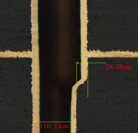
Microsection Diagram